
AI compute capacity is growing exponentially. But as spending on AI chips climbs into the hundreds of billions, the semiconductor supply chain is increasingly strained. To help researchers, policymakers, and the public understand semiconductor inputs and production constraints, we are launching the AI Chip Components explorer.
Building on our AI Chip Sales explorer, which tracks completed chips, the AI Chip Components explorer looks further up the supply chain at the components used to build chips. We estimate how much global chip component supply is consumed by the four leading US AI chip designers: Nvidia, AMD, Google, and Amazon. We further break down the consumption of components by chip type, designer, and quarter. Our scope is limited to the chip itself. We do not cover rack-level components or networking equipment, which are also significant inputs to AI infrastructure.
The explorer tracks three critical chip components
Modern AI chips rely on several specialized inputs: advanced logic wafers that perform the core computation, high-bandwidth memory (HBM) that stores data and feeds it to the compute engines at high speeds, and advanced packaging that integrates logic and memory together. Each is supplied by a small number of upstream manufacturers: TSMC fabricates the logic wafers; SK Hynix, Samsung, and Micron produce HBM; and TSMC packages logic and memory dies together.
Shortages in any one of these can constrain how quickly frontier AI compute scales, shape who gets access to it, and at what cost. These components have become so essential that the firms supplying them — TSMC, Samsung, and SK Hynix — are now the three most valuable companies in Asia, excluding state-owned firms.
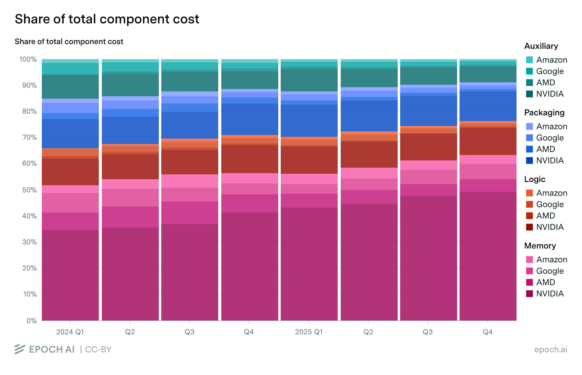
Packaging was the major bottleneck in late 2024 and early 2025
The data reveals several distinct phases of supply chain constraint. The first major bottleneck, from late 2024 to early 2025, was advanced packaging. Today’s leading AI chips rely on TSMC’s chip-on-wafer-on-substrate (CoWoS) packaging to integrate logic dies with HBM stacks. In CoWoS packaging, the logic die and the HBM stacks side-by-side on a silicon interposer, which is a thin silicon wiring layer that allows for dense, short connections between logic and memory. Conventional packaging cannot achieve the interconnect density required for modern AI chips, which is why CoWoS capacity is a critical chokepoint for AI chip production.
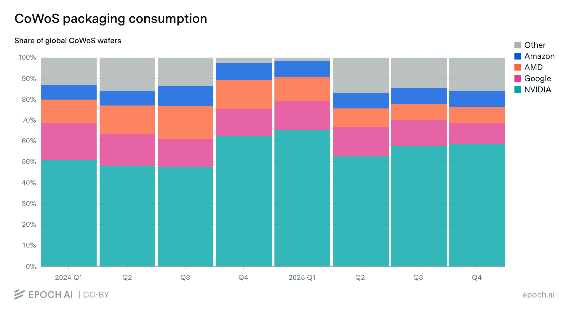
In late 2024 and early 2025, capacity was tight. The top four designers collectively consumed nearly all of TSMC’s CoWoS wafer output, leaving little headroom for other customers. As TSMC expanded its CoWoS capacity through 2025, this bottleneck eased — though the four designers still take roughly 80–85% of total CoWoS supply.
Memory became the bottleneck in 2025
As packaging loosened, HBM tightened. The top four’s share of the global HBM supply jumped sharply in the first quarter of 2025 and has continued to climb.
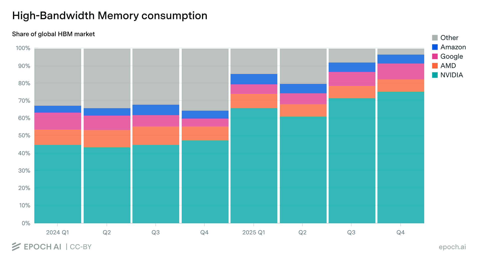
The shift is a result of both the collapse in Chinese demand and a rapid increase in US demand. In 2024, China was a major buyer of HBM. Samsung shipped an estimated 7 million HBM stacks (~$1.4B) to Chinese customers in December 2024 alone. A new round of US export controls then restricted sales to China, effectively closing off the Chinese market. At the same time, the four US designers ramped up chip production of memory-heavy chips like the B300 and TPU v7, increasing their demand for HBM and consuming nearly all of the supply in the second half of 2025.
The memory bottleneck is expected to continue through 2027. HBM supply remains heavily constrained, with all three major suppliers effectively sold out. The shortage is so severe that major customers have reportedly offered to finance SK Hynix’s expansion directly, including by funding new production lines and covering the cost of ASML’s EUV lithography machines.
Advanced logic was a softer constraint in 2024 and 2025
Unlike HBM and advanced packaging, which are produced almost exclusively for AI applications, leading-edge logic wafers serve a much broader market — smartphones, PCs, and networking chips among them. The four designers consumed only ~11% of global leading-edge logic wafer capacity in 2024 and 2025.
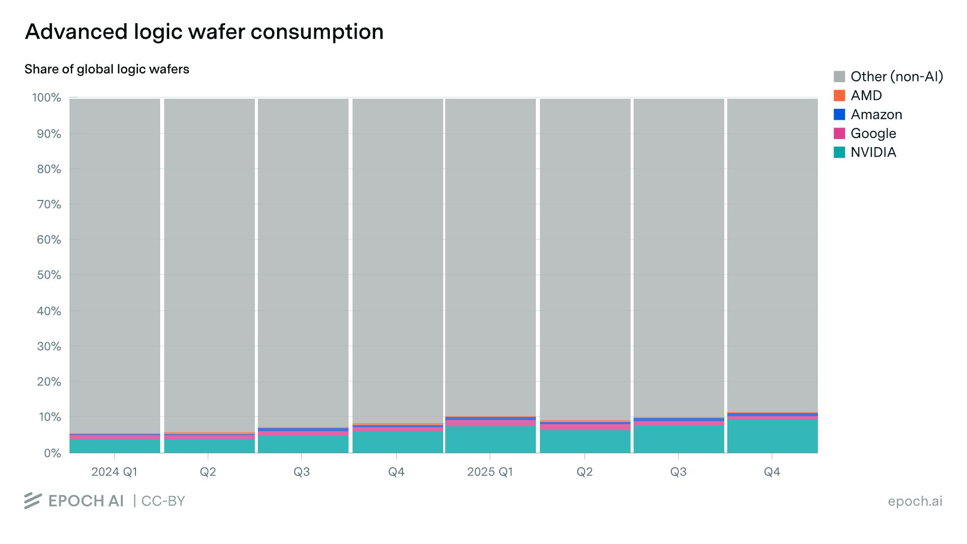
While AI chip production accounted for a relatively small share of demand, the total supply of advanced logic was still heavily utilized. However, compared with HBM and CoWoS packaging, logic supply was likely a softer constraint: AI chip designers could more easily expand their share by outbidding other customers, rather than waiting for entirely new capacity to come online.
Advanced-node capacity is expected to become a more serious bottleneck over the next few years. Next-generation AI chips, such as Nvidia’s Rubin, will shift to the 3nm process, and AI demand will account for a larger share of advanced node capacity.
Chip Component Spend More than Doubled from 2024 to 2025
The component bottlenecks we describe above were driven by rapidly growing demand. Total spending on components across the top four designers more than doubled from 2024 to 2025, rising from $22 billion to $52 billion. HBM drove most of that growth: of the roughly $30 billion year-over-year increase, around $20 billion came from HBM alone.
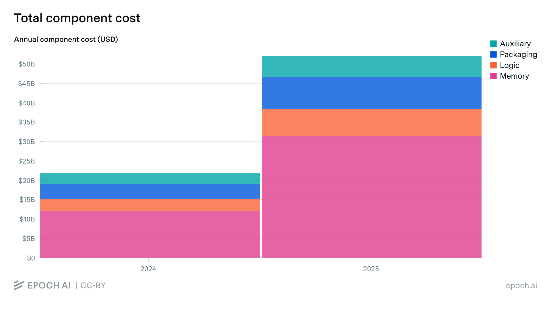
As a result, HBM has become the dominant cost in AI chips. It grew from roughly half of quarterly component cost at the start of 2024 to about two-thirds by the end of 2025. This shift reflects the rising memory content of frontier chips: Nvidia’s B300 carries 288 GB of HBM3E, more than double the 141 GB on the H200, and Google’s TPU v7 follows the same trend.
We hope the AI Chip Components explorer serves as a useful resource for anyone tracking the evolution of the AI compute supply chain. For the full dataset, methodology, and interactive visualizations, visit the explorer.
Thanks to Erich Grunewald, Jack Freed, and Georgia Adamson for their feedback.