
Key Takeaways
- Huawei currently trails Nvidia in both per-chip performance and AI chip production volume. Its most powerful chip, the Ascend 950, delivers roughly half the performance of Nvidia’s H100, which began shipping in 2022, and Huawei will produce less than 4% of Nvidia’s compute output this year.
- Huawei’s published roadmap is ambitious but insufficient given Nvidia’s own progress on per-chip performance. Huawei’s chips will continue to trail Nvidia’s by three to four years until at least 2030.
- HBM is the key bottleneck in Huawei’s production, and China’s domestic manufacturing ramp-up will not be enough to catch up to Nvidia by 2030. If Huawei uses only Chinese-made HBM, its compute output could stay around 1% of Nvidia’s through 2028.
- Smuggling more HBM would improve Huawei’s output, but would not make it competitive with Nvidia. Even if Huawei smuggled 10× as much usable HBM as its entire domestic supply in 2028, its output would still be only about 16% of Nvidia’s.
- Huawei’s constraint starts to move from HBM supply toward per-chip performance by 2028. The gap in usable HBM narrows from 73× in 2026 to 11× in 2028 as domestic Chinese HBM production ramps, while Nvidia’s advantage in compute per GB of memory grows from nearly 3× to 6×.
- LogicFolding is Huawei’s long-term bet for overcoming its per-chip performance disadvantage. By stacking logic vertically, Huawei aims to increase planar transistor density despite being stuck on 5–7 nm-class processes, but the first Ascend chip using LogicFolding won’t arrive until 2030.
Overview
The US-China AI competition runs the entire technology stack, from applications and models to data center infrastructure, chips, and semiconductor manufacturing equipment. Chips and manufacturing equipment form the foundation of that stack and determine how much compute each side can field, which will have significant implications for the competition for years to come.
This is why semiconductor export controls have been a centerpiece of US AI policy, and why so much depends on how China’s homegrown chip industry stacks up against America’s. As China’s leading AI chip designer, Huawei is a useful proxy for China’s progress toward indigenizing AI compute production.1
Huawei laid out its chip roadmap in a keynote at IEEE ISCAS 2026 and showcased an accelerated version at its 2026 annual conference. The roadmap is ambitious: it plans to pack more compute into each chip, connect far more chips into a single high-speed system, and mature the software that determines how much of that hardware is actually used. But Nvidia continues to push the frontier, claiming its new Rubin architecture delivers 5.4× the performance per megawatt of its predecessor, Blackwell, and the upcoming Feynman generation is set to push that further in 2028. With Nvidia making strides, can Huawei close the gap?
Total compute is a function of both per-chip performance and the number of chips produced. Huawei currently lags Nvidia on both, and US export controls constrain its ability to improve either.
In the near term, limited supply of high-bandwidth memory (HBM) is the binding constraint on Huawei’s production. Even after supplementing domestic HBM with stockpiles of foreign HBM, lower-bandwidth memory alternatives, and smuggled HBM, we estimate Huawei will produce less than 4% as much AI compute as Nvidia in 2026. Using only Chinese-made HBM, its output could remain around 1% of Nvidia’s through 2028.
As Chinese HBM production ramps through 2030, the memory supply gap narrows, but the weaker per-chip performance of Huawei’s chips becomes a comparable constraint. Huawei’s chips will continue to trail Nvidia’s by roughly three to four years through 2030. Nvidia is pursuing the same levers to improve chip performance, and compounding that progress with denser process nodes that Huawei cannot access. Even if Huawei delivers on its roadmap and China’s memory makers hit their expansion targets, it will not be enough to close the gap this decade.
Huawei’s long-term bet to improve chip performance is LogicFolding, a technique that vertically stacks active logic layers to reach the transistor density of a far more advanced process node. But the first Ascend chip to use it is set to arrive in 2030, two years after Nvidia’s Feynman is expected to ship with stacked logic on a 1.6 nm-class process.
The rest of this report works through this in turn: where Huawei stands in 2026, why its roadmap will fail to close the performance gap, why greater domestic memory production will not be sufficient to make up the chip volume gap, and what Huawei’s bet on LogicFolding could mean for the years beyond 2030.
This report assumes some familiarity with AI chip terminology. A short walkthrough of the relevant chip structure follows for readers who want it. Read more: Anatomy of an AI chip
The term “chip” is used loosely: it can refer to an individual piece of silicon, called a die, or to the complete packaged device.
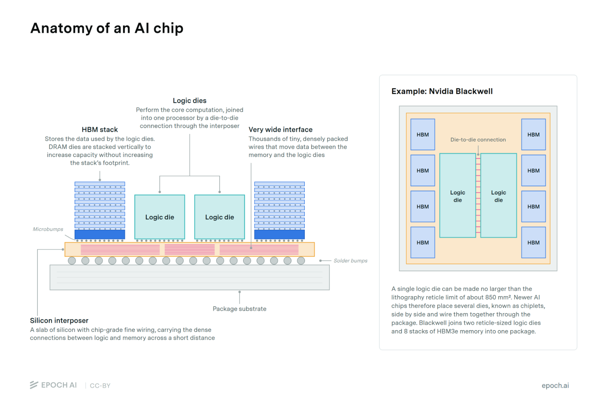
The two core components of a chip are logic and memory. The logic die performs the core computation, while the high-bandwidth memory (HBM) stores data and moves it into and out of the logic die. A logic die’s performance depends on how many arithmetic units it contains, how quickly they operate, and how effectively the chip can keep them supplied with data. Those factors are shaped by the size and number of logic dies, the chip’s architecture, its clock speed, memory and interconnect bandwidth, power budget, and the process node, which determines how densely transistors can be packed.
HBM is memory built by stacking DRAM dies on top of one another. Vertically stacking dies is a complex back-end process, but leading AI chips rely on it since stacking provides significantly more capacity per package footprint. The HBM sits beside the logic die, and the two are linked through a very wide interface that moves data at immense bandwidth, which requires thousands of tiny, densely packed wires. To accommodate this, the logic dies and HBM sit on an interposer, which is usually a passive silicon die with dense copper routing. The short connections and thousands of data paths provide far more bandwidth than conventional DDR connected through a circuit board.
The interposer determines how much silicon can be placed in a single package. A single logic die can only be made so large (~850 mm²), so to pack more compute into one package, newer AI chips place several dies, or chiplets, side by side and wire them together through the interposer. Nvidia’s Blackwell, for example, joins two large logic dies with 8 stacks of HBM into a single GPU.
Huawei’s starting position in 2026
The primary metric we use to compare Huawei and Nvidia is the effective amount of compute each produces. Below, we look at the two components of that metric, performance and production volume, then combine them.
Hardware performance
The flagship AI chip that Huawei will produce in 2026 is the Ascend 950. The 950 comes in two variants: the 950PR and 950DT.
The 950PR is optimized for prefill — the more compute-intensive stage of inference — and delivers 2 PFLOPS of FP4 performance with 128 GB of Huawei’s custom memory and 1.6 TB/s of memory bandwidth.
The 950DT, which is slated for Q4 2026, shares the same compute die as the 950PR, but comes with greater memory capacity and bandwidth: 144 GB and 4 TB/s. Read more about Huawei’s design choices for the 950
Huawei’s design choices for the Ascend 950 are notable.
First, Huawei shrank the logic footprint relative to the 910C, its most capable AI chip in 2025, from two ~665 mm² logic dies to two ~400 mm² dies. The likely reason is yield; many of the 910C logic dies reportedly came from TSMC, while the 950 is expected to depend much more heavily on fabrication from SMIC, China’s leading semiconductor foundry. Since defect density is uniform, yield degrades exponentially as die area increases, making large dies especially costly on a less mature process. Huawei therefore likely chose smaller chiplets to improve yield and make mass production more economical.
Second is Huawei’s memory choice for the 950. Huawei has limited access to HBM. CXMT, China’s largest memory manufacturer, is ramping HBM production, but at the start of 2026 its HBM output was too limited to support hundreds of thousands of Ascend chips. However, CXMT was producing meaningful amounts of LPDDR, which is a lower-cost, lower-bandwidth memory alternative.
The 950PR, which was in mass production in Q1 2026, likely uses a non-HBM DRAM solution with characteristics closer to LPDDR. This is further supported by a purported image of the 950PR, which shows two compute dies in the center, flanked by what appear to be I/O dies. The large modules above and below the compute dies seem to be memory, but sit too far from the compute dies for HBM, and instead suggest LPDDR. It’s also possible that CXMT designed a custom DRAM/hybrid HBM solution for Huawei rather than following a standard JEDEC DDR or LPDDR spec. If Huawei designed the 950PR around memory from a single supplier such as CXMT, there would be less reason to conform to an industry-standard interface. The tradeoff with using non-HBM memory is reduced bandwidth. While both the 910C and 950PR have 128 GB of memory capacity, the 910C has double the memory bandwidth.
The memory constraints explain why Huawei designed the 950PR specifically for prefill. Prefill is the more compute-intensive stage of inference and is less constrained by memory bandwidth than decode. It performs more computation per byte of communication, so a lower-bandwidth chip imposes a smaller performance penalty. The decode stage of inference is more bandwidth-intensive, since it involves reading the model weights and KV cache repeatedly.
Huawei uses the more available yet lower-bandwidth memory for prefill while keeping scarce HBM for the 950DT, which is specialized for workloads where the additional bandwidth matters most for performance. The 950 production timeline also fits with this theory: the 950PR was in volume production at the beginning of 2026 when CXMT HBM output was extremely limited, and mass production of the 950DT will likely start in the second half of 2026 as CXMT expands HBM production.
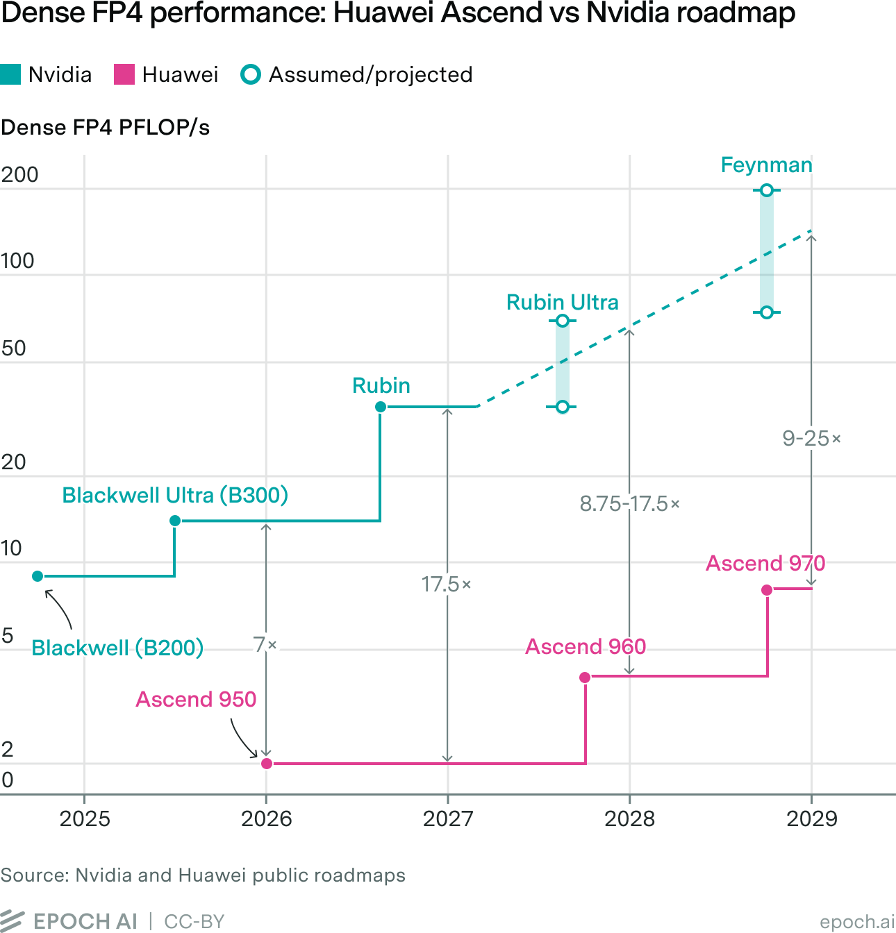
On performance, the 950 trails Nvidia’s B300.2 The B300 has a theoretical peak of 13.5 PFLOPS at FP4 versus 2 PFLOPS for the 950, a 6.75× gap. The gap is due to differences in the logic die area, transistor density, and other factors such as tensor-core design, clock speed, power envelope, and datapaths. Read more about the performance comparisons
On performance-per-dollar, the gap narrows. At 13.5 PFLOPS and roughly $40,000, the B300 delivers 0.34 TFLOPS per dollar, compared with 0.05 for the 950DT at 2 PFLOPS and $37,000.
The performance-per-dollar gap is about 6.2×, which is tighter than the 7× on-paper compute gap. However, memory bandwidth (rather than FP4 performance) may be the more appropriate measure for bandwidth-bound workloads. On bandwidth per dollar, the B300 delivers 0.2 GB/s per dollar versus the 0.11 GB/s per dollar for the 950DT.
Across all of these metrics, the performance gap in deployment is likely wider than the on-paper specs suggest because Nvidia’s more mature software delivers higher utilization.3

The Ascend chips significantly lag in both arithmetic performance and memory bandwidth. The Ascend 950DT delivers 1 PFLOP/s of FP8 performance, which is roughly half of the Nvidia H100, and has comparable memory bandwidth to the H100. In other words, Huawei’s latest and most powerful GPU delivers only half the arithmetic performance of a two-generation-old Nvidia chip that first started shipping in 2022, suggesting that Huawei’s chip performance currently trails Nvidia by four years.
Huawei’s chips are weaker, but its scale-up systems are larger. Last year, Huawei introduced the CloudMatrix 384, a scale-up system that connects 384 Ascend chips across 16 racks into a single high-bandwidth domain, compared with the 72 GPUs in Nvidia’s NVL72 rack. This reflects Huawei’s broader strategy: where each chip falls short individually, connect more of them together and make up the difference in aggregate. It is arguably the area where Huawei is most competitive with Nvidia today.
Production volume
Huawei also currently trails Nvidia in chip production. We estimate Huawei produced 800,000 Ascend units in 2025, compared to the 4.5 million units Nvidia sold. For 2026, our median estimate is that Huawei will produce 1.5 million units vs. 5.9 million for Nvidia.
Much of the Ascend production to date has also relied on foreign components. A teardown found that Huawei’s leading chip last year, the Ascend 910C, used logic dies fabricated by TSMC and HBM from Samsung/SK Hynix. Across 2024 and 2025, Huawei stockpiled and smuggled large amounts of logic wafers and HBM.4 Much of that stockpile was spent on 2025 Ascend production, and we model it being fully spent in 2026.
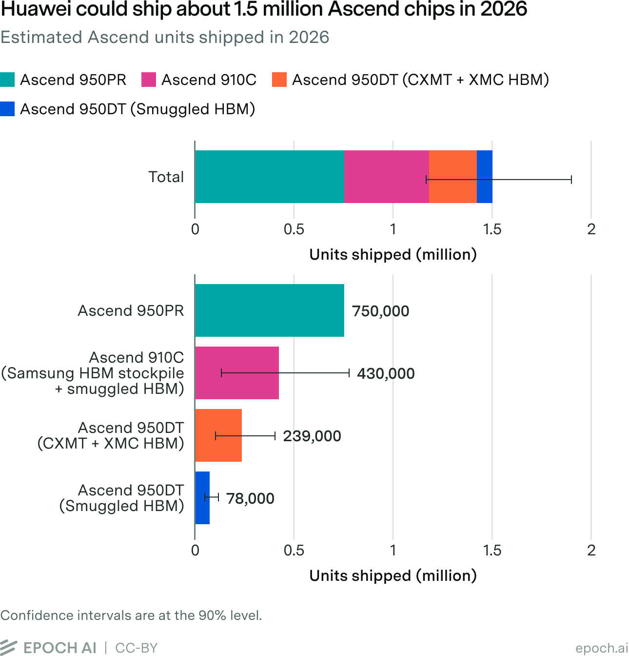
Our 2026 estimate comes from modeling each memory supply channel: the 1.5 million units are spread across a mix of the 950PR, 950DT, and 910C, and are far above what domestic production of HBM alone could support. Our median estimate aligns closely with a report from the Wall Street Journal that Huawei expects to ship 1.5 million Ascend units in 2026. Read more about Huawei’s production and memory-supply mix for 2026
Each Ascend chip type has a different memory source. Tom’s Hardware reported that Huawei plans to ship 750,000 units of the 950PR in 2026. The memory for the 950PR is LPDDR rather than traditional HBM and could be sourced from CXMT, which had strong enough production volumes of LPDDR by early 2026 to support hundreds of thousands of 950PR units. Additionally, we estimate that Huawei’s remaining stockpile of Samsung HBM from the end of 2024 plus smuggled HBM in 2025 could support roughly 430,000 additional Ascend 910Cs.5 The stockpiled Samsung HBM was largely 8-high HBM2E, which does not fit the chip architecture, memory capacity, or bandwidth specs of the 950DT. But, we know that the 2025 Ascend 910C used the Samsung HBM and thus Huawei would likely use the rest of the stockpile to produce additional 910C units.
That leaves the 950DT, which could use CXMT-produced or smuggled HBM.6 Our median estimate suggests that CXMT and XMC together supply enough HBM for approximately 240,000 units of the 950DT 96GB variant.7
Adding our estimates of the three chips gives a median of 1.5 million Ascend units: 750,000 950PRs using non-HBM memory, 430,000 910Cs using the remaining stockpile and HBM smuggled in 2025, 240,000 950DTs using CXMT and XMC HBM, and 80,000 950DTs using smuggled HBM. This precise mix is uncertain, but our median estimates are based on the product and memory-supply mix Huawei had access to.
Compute output
The chip counts above do not translate directly into compute, since each chip type varies significantly in performance. To measure the effective compute each company produces, we take the total processing power (TPP) of each chip, expressed as the equivalent number of Nvidia H100 GPUs, and multiply this ratio by the number of chips. H100-equivalents (H100e) provide a way to measure chips and output on a common scale.
Huawei’s estimated 2026 production of 1.5 million units translates to 880,000 H100-equivalents (H100e) of compute. Nvidia’s 5.9 million chips, primarily Blackwell Ultra and Rubin GPUs, have far greater per-chip performance and thus translate to 23 million H100e. Even though Huawei’s shipments would nearly double from 800,000 in 2025, its output would represent less than 4% of the compute we estimate Nvidia will ship in 2026; even at the extremes of our confidence intervals, Huawei’s share would only reach 6%.
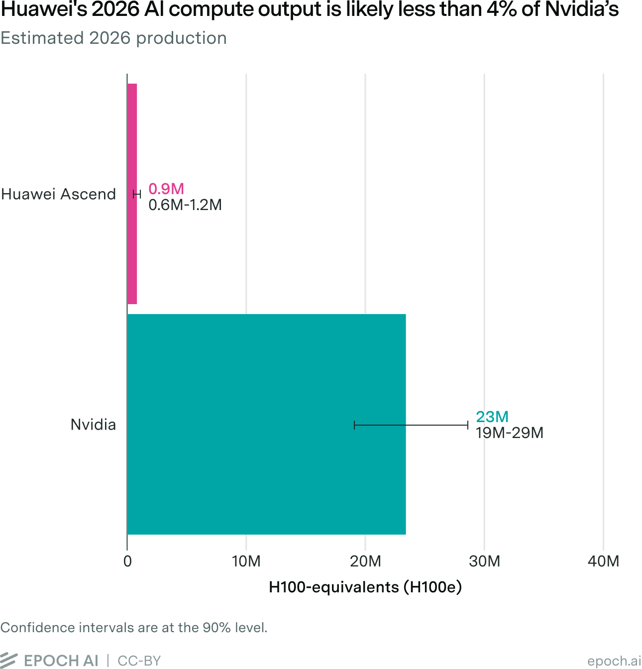
We estimate Huawei’s production volume of Ascend chips is one-fourth of Nvidia’s, and its chips deliver roughly 7× less compute on paper. These effects compound, leaving Huawei producing roughly 25× less compute than Nvidia in 2026.
The H100-equivalent measure is an on-paper comparison, however: it does not account for memory, scale-up domain, workload shape, interactivity, software, and other factors, each of which can affect the performance realized in deployment. Today, Huawei’s realized performance is likely lower than the H100-equivalent measure suggests, due to its CANN software stack being far less mature than Nvidia’s CUDA. We look more closely at how Huawei could compete on software and scale-up domain below.
Huawei’s roadmap to improve performance by 2030
Huawei has laid out an ambitious roadmap to improve performance. Like all major chip designers, it is focused on optimizing the entire computing system, rather than just the individual chip. Huawei calls this “Tau Scaling”, where tau is the time cost of moving and computing data.
The time required to finish an AI workload depends both on how quickly the chips can process data and on how efficiently their compute units are utilized. Training frontier models requires tens of thousands of AI chips. At that scale, communication overhead grows, and the compute engines within a chip sit idle waiting for data, which reduces the fraction of peak performance that is realized.
This gives chip designers two ways to reduce time cost: increase the computational performance of each chip, and reduce the time chips spend underutilized. The first increases the aggregate compute performance of the system, and the second increases the fraction of the theoretical compute capacity actually used.
Huawei’s near-term roadmap projects gains on both fronts. To raise per-chip performance, it plans to improve the compute and memory performance of each chip; to raise utilization, it plans to connect more chips with a faster fabric into a single domain and design better software. We take each in turn.
More performance per chip
Huawei’s chips already trail Nvidia’s substantially, so narrowing the per-chip gap is necessary both to increase Huawei’s total compute output and to reduce how heavily it must rely on system-level scaling.
There are four standard ways to improve the computational performance of a chip: (1) increase transistor density, (2) make each die larger, (3) place more dies side by side in a single package and (4) optimize the chip’s architecture. Importantly, the gains from all four compound. A more advanced process node packs more compute onto a given surface area; a larger die scales that density across more surface area; a larger package allows for more logic dies and HBM; and architectural optimizations increase the performance extracted from that silicon.
Transistor density
Huawei’s fabrication partner, SMIC, however, can’t make transistors nearly as dense as TSMC can. US export controls restrict sales of advanced lithography machines to China, and China’s indigenous efforts to produce these machines likely won’t materialize until after 2030, which leaves SMIC unable to print transistors denser than a 5 nm equivalent process until at least the end of the decade. SMIC could scale further with DUV, but that would require increasingly complex multipatterning, lowering throughput and raising costs and process risk.
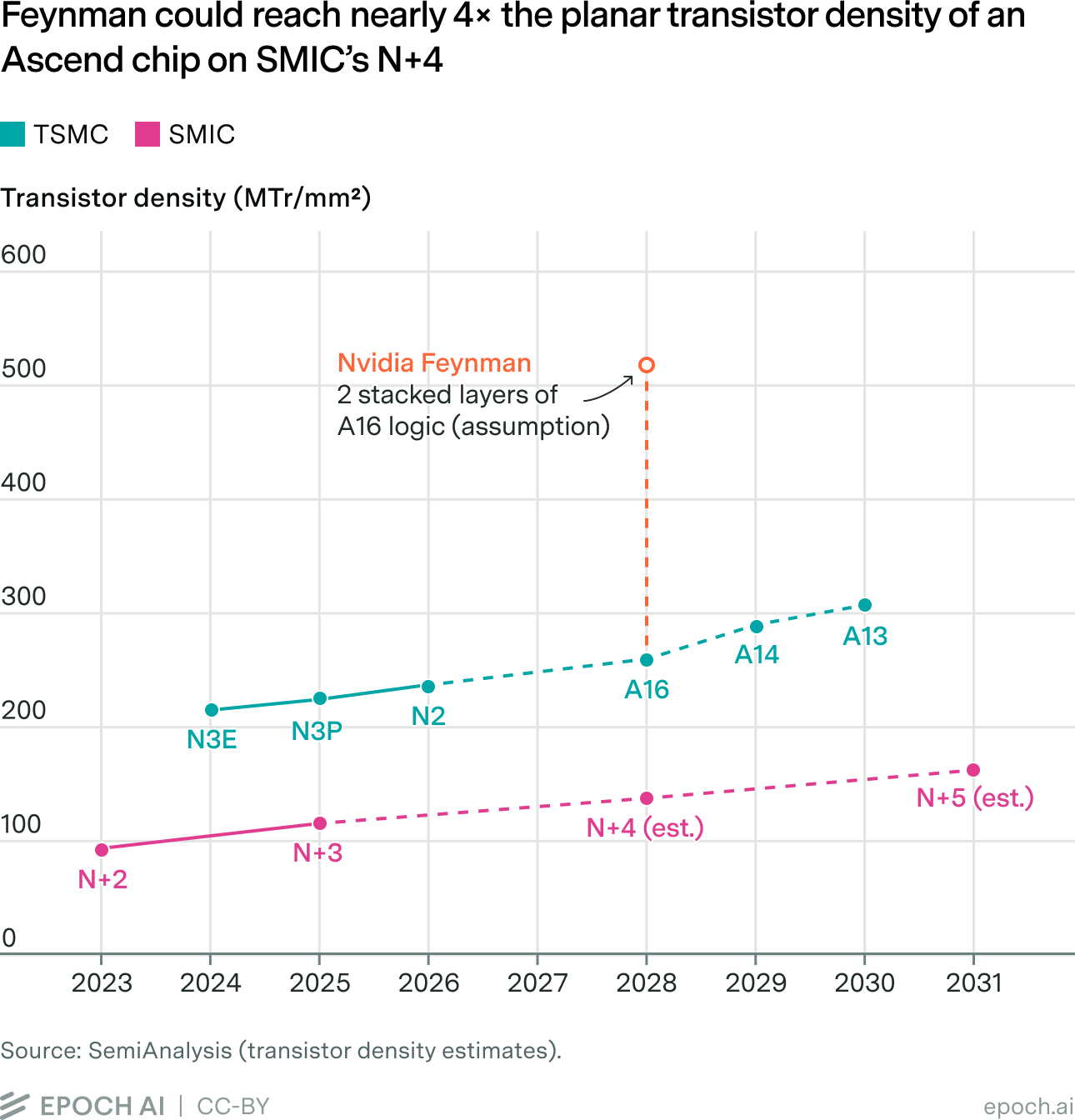
Nvidia, by contrast, has a roughly 2× advantage in transistor density, and that gap will persist through 2030. The Rubin GPU will be fabricated on TSMC’s N3P process node, which delivers roughly 224 million transistors per square millimeter (MTr/mm²). SMIC’s leading process in mass production is the 7 nm N+3 node. It delivers 113 MTr/mm², which achieves only half the density of TSMC’s N3P.
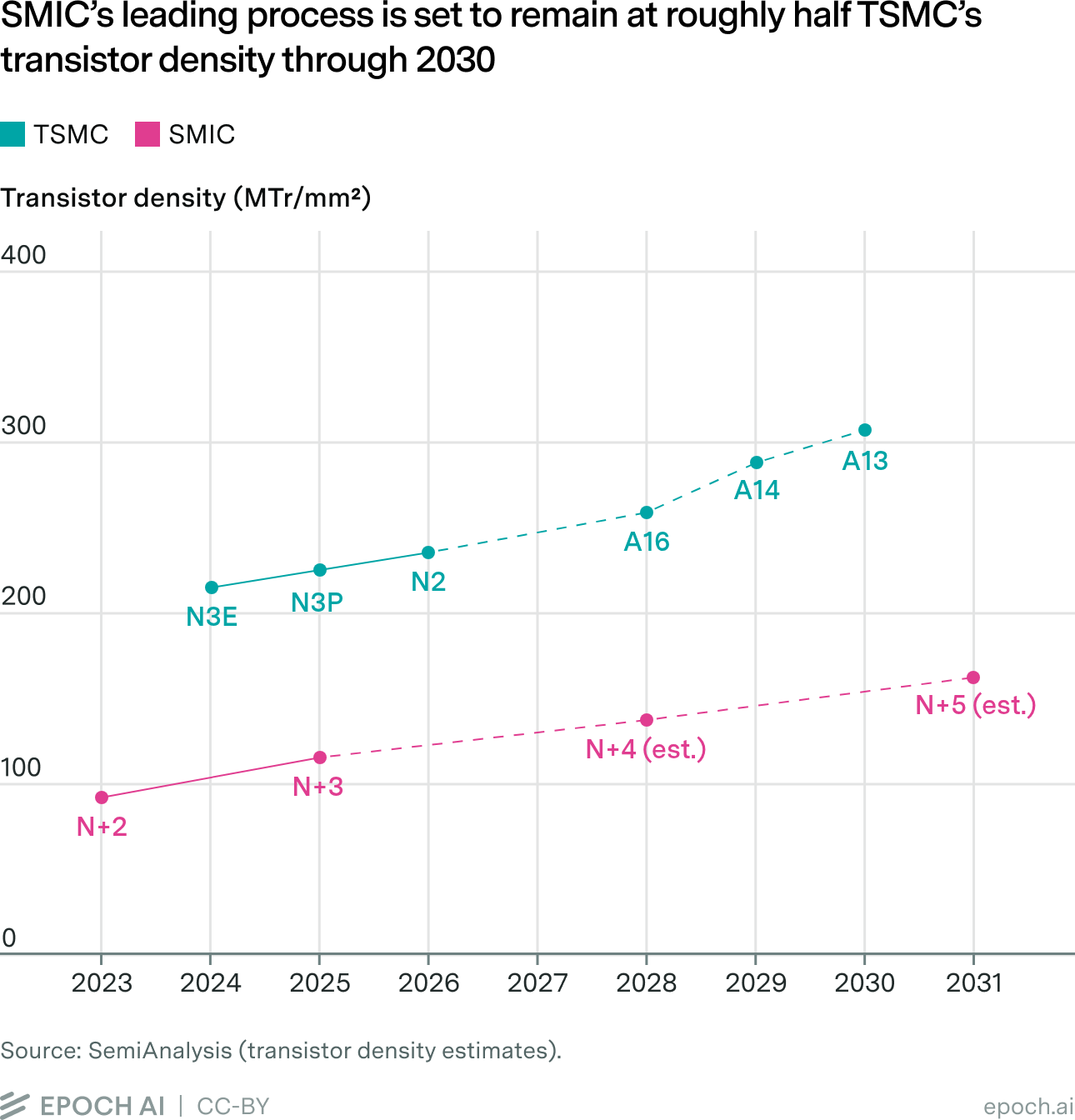
TSMC is aiming to bring its 1.6 nm-class A16 process to production by 2028, followed by its 1.4 nm-class A14 process by 2029. SMIC will move to its N+4 and N+5 nodes over the next five years, but at each point in time, TSMC’s leading process will deliver roughly double the transistor density of SMIC’s.
Nvidia’s next generation of GPUs, Feynman, is expected to start shipping in 2028 and will utilize TSMC’s A16 process. All else held equal, this would give Feynman a baseline advantage of 2× over the Ascend 970, which ships in late 2028.
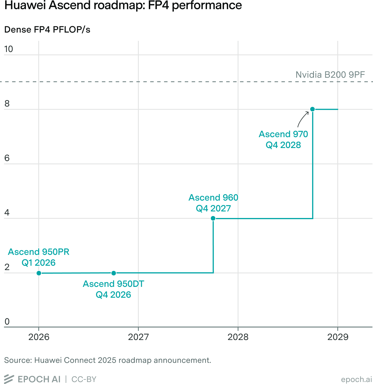
Huawei’s roadmap nonetheless projects a 7× increase in compute over two generations — from the Ascend 950 to the Ascend 970 in 2028. That 7× improvement cannot come from a more advanced process node. The compute dies in the 950 and 960 are fabricated on SMIC’s N+3 process, while the 970 likely moves to the more advanced N+4 process. Both are 5–7 nm equivalent DUV processes, and the transition to N+4 is expected to increase transistor density by only 20%. Huawei will therefore have to obtain most of the projected 7× gain from the other three ways: larger dies, more dies per package, and architectural changes such as its shift toward 4-bit arithmetic. In other words, Huawei’s near-term performance roadmap is a packaging and architecture roadmap rather than a process-node roadmap.
Packaging
Huawei can compensate for a less advanced front-end process by using a more advanced back-end process. The Ascend chips could use larger dies and integrate more silicon into each package, but this comes with tradeoffs. Larger dies are more likely to contain a defect, reducing the number of usable dies per wafer. Larger packages must successfully integrate more chiplets, memory stacks, and I/O, increasing manufacturing complexity and creating more opportunities for a packaging failure. As package size grows and holds more logic and memory, it carries more economic value and each failed package thus imposes a larger cost.
Whether Huawei can meet its roadmap goals will depend heavily on the capabilities of its back-end manufacturing partners. If they cannot maintain yields at any one of these steps, it would threaten both Huawei’s production volume and unit economics.
Nvidia is expanding package size as well, packing more silicon into each chip: Blackwell has two reticle-sized compute dies, while Rubin disaggregates I/O onto separate chiplets, freeing up more of the compute die area for arithmetic logic units.
TSMC’s CoWoS roadmap progresses from 5.5×-reticle packages in 2026 to 9.5× in 2027 and 14× in 2028, allowing Nvidia to place more compute, memory, and I/O in each package with every generation.
Chip architecture
Huawei’s updated Ascend roadmap prioritizes performance at 4-bit numerical formats as opposed to higher-precision formats such as 16-bit. Optimizing for lower precision significantly increases the number of operations per second the hardware can perform since the simpler 4-bit format allows more calculations to be performed with the same amount of silicon. Huawei, recognizing that frontier inference and training workloads are moving towards 4-bit precision, has likely rearchitected its chip to allocate more silicon to low-precision arithmetic units and thus significantly improved the Ascend’s performance running frontier AI workloads. In doing so, Huawei raised the FP4 performance of the Ascend 970 from 8 PFLOP/s to 14 PFLOP/s, and projected an impressive 28 PFLOP/s for its 2029 Ascend 980.
Vertical stacking
Packaging improvements, however, do not provide a long-term solution to the density ceiling itself. To that end, Huawei plans to begin stacking logic dies vertically to fit far more transistors within a given footprint than SMIC’s process can print in a single layer. However, this technique, which Huawei calls LogicFolding, won’t reach the Ascend line until the end of this decade. We discuss its post-2030 implications at the end of this report.
Nvidia is adding that dimension sooner. Its Feynman generation, expected in 2028, will reportedly use 3D-stacked dies fabricated on TSMC’s A16 process node.8 In other words, Feynman stacks at least two layers of logic fabricated on a 1.6 nm-class process in 2028, two years before the first folded Ascend, whereas the most advanced process that the Ascend chips could utilize is SMIC’s N+4.
Feynman stacking two layers of 1.6 nm logic would give it the equivalent planar density of over 500 MTr/mm² compared to the Ascend’s 137 MTr/mm² on SMIC’s N+4. While the planar density gap achieved by each process is only 2×, by adding another dimension to scaling, Nvidia’s Feynman compounds the transistor density advantage and grows the gap with Ascend to nearly 4×. The larger packages on TSMC’s roadmap would then let Nvidia place more of those stacked dies side by side, compounding vertical stacking and denser dies with horizontal scaling.
Memory
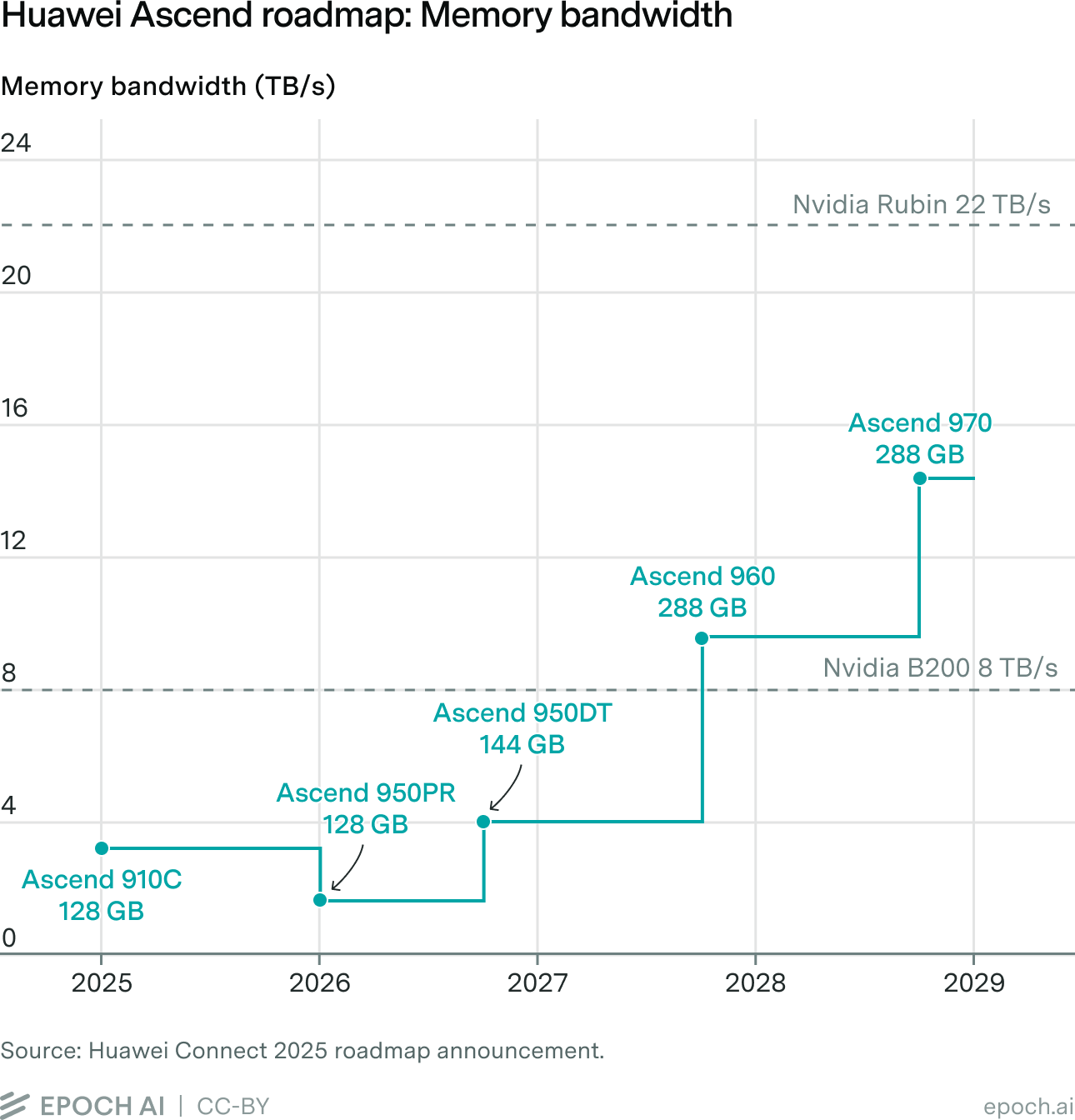
Per-chip performance also depends on the memory that feeds the logic die. Huawei’s access to memory is similarly constrained by the production capacity and performance of domestic HBM solutions, which currently lag the frontier by two generations. However, Huawei projects that memory bandwidth per chip will increase from 4 TB/s on the 950DT to 14.4 TB/s on the Ascend 970, which ships in Q4 2028. This suggests that Huawei believes its memory suppliers will develop HBM solutions that are between HBM3E and HBM4 in performance by the end of 2028.9

Nvidia’s memory solutions are advancing too. Memory bandwidth increases from 8 TB/s on Blackwell to 22 TB/s on Rubin. Nvidia is developing custom HBM base dies that move some memory-control logic from the compute die to the memory stack, freeing up compute die area and minimizing data movement. Nvidia claims that its custom HBM base dies result in 30% more memory bandwidth than HBM4E, 15% less HBM power consumption, and 25% more compute die area available. HBM stacks are also growing, with 20-layer stacks on the roadmap and longer-term plans to stack memory directly on top of logic. TSMC’s A16 node will also introduce backside power delivery in 2027, which leaves more space for signal wires on the face of the die.
Limited access to technology and key components forces Huawei to optimize under greater constraints. Huawei uses complex multipatterning just to achieve the density of a 5–6 nm process, while Nvidia achieves superior transistor density from the process node alone and then compounds that advantage by vertically stacking those dense dies and placing more of them in a single package. This is the compounding effect that Huawei can’t keep up with.
Huawei will remain three to four years behind in chip performance
On paper, Nvidia’s B300 already delivers roughly 7× more raw arithmetic performance than Huawei’s Ascend 950 series. As Nvidia moves from Blackwell to Rubin and Rubin Ultra, that point-in-time gap will hold. The first Ascend chip expected to come close to the B300 in peak performance is the 970, slated to ship in late 2028. Given that the B300 arrived in 2025, that would put Huawei roughly three to four years behind Nvidia at the chip level even out to 2029.
Larger systems
Huawei is arguably most competitive in large-scale systems and networking. It may not need to achieve parity with Nvidia on a per-chip basis if it can build a sufficiently good system around those chips.
Both companies build scale-up domains, where their fastest networks connect a set number of chips. Nvidia places enormous bandwidth inside a relatively small, uniform 72-GPU domain and relies on software to keep communication-intensive work within the rack.10 Huawei’s strategy is to compensate for weaker per-chip performance by pushing the scale-up boundary for its domains much further, and it plans to ship “SuperPoDs” this year that connect up to 8,192 chips.
| Scale-up domain | Chips per domain | Per-chip link | Fabric | Timing |
|---|---|---|---|---|
| Huawei CloudMatrix 384 | 384 | 0.4 TB/s11 | Optical | Shipping |
| Huawei Atlas 950 SuperPoD | 8,192 | 1.0 TB/s12 | Optical | Q4 2026 |
| Huawei Atlas 960E SuperPoD | 4,096 | 1.1 TB/s13 | Optical | Q1 2027 |
| Nvidia NVL72 (Blackwell) | 72 | 0.9 TB/s14 | Copper | Shipping |
| Nvidia NVL72 (Rubin)15 | 72 | 1.8 TB/s | Copper | H2 2026 |
| Nvidia NVL576 (Rubin Ultra) | 576 | 1.8 TB/s | Copper + optical | 2028 |
However, 72 and 8,192 aren’t directly comparable. Nvidia builds a fabric that allows any chip to communicate with any other chip at full bandwidth. Huawei, however, can’t build a non-blocking fabric that handles simultaneous communication from thousands of chips, forcing it to introduce a communication hierarchy, which makes performance more dependent on where chips sit in the network, the workload shape, and the software quality. While greater aggregate bandwidth and compute are beneficial for workloads such as wide expert parallelism, it can lead to significant communication overhead based on the communication patterns of the workload. Huawei can combat these tradeoffs with capable software, innovative network topologies, and strong design choices, in which case it could utilize the aggregate performance of its SuperPod and deliver competitive performance. However, Huawei doesn’t currently publish the key performance metrics needed, such as bisection bandwidth and pairwise bandwidth, to assess how competitive its ambitious scale-up solution is.
Nvidia could also build a scale-up fabric that extends to thousands of GPUs, but implementing a hierarchy like Huawei’s would mean accepting location-dependent performance, forfeiting a non-blocking fabric, and greater software complexity. The hardware complexity would grow as well since connecting many chips together would require more switches, ports, and optical modules, which consume more power and floor space, and fail more frequently than a rack of 72 chips. Since Nvidia’s stronger GPUs are able to keep much of the communication-intensive work inside a 72-GPU domain, it has less reason to make those tradeoffs.
Nvidia is nonetheless expanding at the rack level. The total rack bandwidth doubles with each generation from 130 TB/s with Blackwell to 260 TB/s with Rubin to 520 TB/s with Rubin Ultra. The scale-up domains are also growing in size: Rubin Ultra scale-up systems expand to 144 and 576 GPU configurations by connecting multiple racks, with copper inside each rack and optics between racks. However, recent reporting suggests that the denser Rubin Ultra racks have slipped to 2028. With Feynman, the scale-up domain could increase to 1,152 GPUs connected over eight racks each holding 144 GPUs.
Manufacturing and assembling a massive pod system containing thousands of chips is an under-appreciated challenge. Nvidia experienced manufacturing challenges even with Blackwell’s smaller 72-GPU rack. Handling a pod with 100× more chips only exacerbates these challenges. Read more about how Nvidia and Huawei design their scale-up domains
Nvidia concentrates bandwidth inside the rack
Nvidia’s strategy is to build a relatively small but extremely strong scale-up domain and orchestrate workloads to stay within the rack as much as possible. Within a GB300 NVL72 rack, each GPU can send an aggregate of 900 GB/s to all other GPUs and receive another 900 GB/s. The shared network within the rack is large enough to allow all 72 GPUs to transmit data simultaneously at full bandwidth. This guarantees that communication will not be bottlenecked by the shared network and gives each GPU constant and predictable access to the rest of the rack.16
Once traffic moves off the rack, it travels through a separate network at 100 GB/s per chip, a 9× drop in bandwidth.17 Nvidia could try to preserve bandwidth at the rack-to-rack level, but doing so would come with steep tradeoffs including more switches, cabling, power consumption, rack complexity, and cost.18 Instead, Nvidia accepts the bandwidth cliff and relies on software to keep the communication-intensive work inside the rack.
Huawei pushes the scale-up boundary further
Last year, Huawei introduced the CloudMatrix 384, its scale-up solution that extends to 384 chips across 16 racks.19 Huawei achieved a non-blocking fabric delivering 400 GB/s per chip by using copper within a rack and optical connections for rack-to-rack communication. Once the data traffic leaves the CloudMatrix 384 domain, it flows through a separate RDMA scale-out network.
Huawei will soon ship its SuperPoD solution that connects 8,192 chips. However, Huawei cannot maintain a non-blocking fabric at this scale and instead must introduce a communication hierarchy. Its UB-Mesh design connects 64 chips within a rack, 16 racks within a 1,024-chip pod, and then 8 1,024-chip pods through another layer of switches to reach 8,192 chips. Traffic between two neighboring chips differs substantially from traffic flowing from one end of the SuperPoD to the other. Neighboring chips will have the shortest and strongest connections, while the distant traffic passes through shared and possibly congested parts of the network.
The communication hierarchy also changes what Huawei’s 1 TB/s unidirectional bandwidth-per-GPU figure measures. Unlike Nvidia’s non-blocking fabric, Huawei’s 1 TB/s figure represents the amount of data each chip can inject into the shared network, rather than a guaranteed bandwidth from one chip in the pod to every other chip. Communication with a distant chip would pass through multiple hops, any of which could be narrow and congested. Injection bandwidth alone provides little information about performance when a workload is distributed across the entire pod.
When is a large scale-up domain useful?
Adding chips only helps if the workload can be organized so that the heaviest communication stays local. If the software is successful, the system can combine weaker processors into a cohesive whole. If orchestration and workload compatibility are poor, however, data will repeatedly cross shared portions of the network, increasing congestion and limiting the benefit of aggregating compute.
Wide expert parallelism (wide EP) is one workload shape that could benefit from Huawei’s large pods. A sparse mixture-of-experts model contains many experts but routes each token to only a few. Spreading those experts across more chips gives the model access to more memory and allows each chip to hold and run fewer experts. This helps compensate for each Ascend chip’s lower individual performance. The lower chip-to-chip bandwidth in the SuperPods could also matter less with wide EP. Wide EP is communication intensive but the size of each message is very small and, according to Huawei, 96% of the messages are two bytes. Given the small message size, the traffic is limited more by how fast a chip can send and receive messages rather than how wide a single link is, which accommodates the specs of the SuperPod well.
The tradeoff is increased communication overhead, which needs to be appropriately managed. If Huawei can develop software that efficiently orchestrates the workload and keeps expert traffic local, then wideEP could mitigate the per-chip disadvantages Huawei faces and utilize the greater aggregate compute and bandwidth of the SuperPod.
Scale-up is a meaningful way for Huawei to mitigate the impact of weaker chips, but it is not a substitute for closing the per-chip performance gap. A larger scale-up domain can aggregate enormous amounts of compute and memory, but introduces greater communication, software complexity, power consumption, and reliability issues. Huawei’s system-level engineering could credibly narrow the realized performance gap, but the evidence or results from production workloads are insufficient to assume that it erases the underlying hardware disadvantage.
Better software
Software determines how workloads get parallelized, how communication is overlapped with computation, how memory is managed, and ultimately how efficiently the hardware is utilized. Two chips with similar on-paper specifications can deliver very different observed performance depending on their software quality. Even on identical hardware, the inference framework alone can move realized performance by more than an order of magnitude.20
Software is therefore its own lever in determining hardware performance and one of Nvidia’s strongest. Huawei’s equivalent of Nvidia’s CUDA is called CANN, which was first released in 2018 and is far less mature and makes working with Ascend GPUs difficult. When DeepSeek tried to train its R2 model on Ascend, Huawei sent its own engineers in and still couldn’t complete a training run, prompting DeepSeek to revert to Nvidia.
While CANN is currently less mature than CUDA, it has a viable path to being competitive. Much of Nvidia’s software advantage comes from a feedback loop with frontier AI companies, who push the hardware to extremes and expose bottlenecks in kernels, compilers, memory management, model sharding, and collective communication. Nvidia can then address those bottlenecks through software and also accordingly optimize the architecture of its next generation of chips.
Chinese AI labs could create a similar flywheel for Huawei. Compute scarcity gives them a strong incentive to optimize close to the hardware, while export controls push more workloads onto Ascend. Those workloads would expose bottlenecks, generating feedback that could improve CANN and give Huawei earlier insight into frontier model architectures. Better hardware and software would then help Chinese labs push the frontier, generating more useful feedback and creating a flywheel.21 Chinese labs may also be more willing than closed-source Western labs to share architectural details with Huawei and contribute back to the ecosystem given both their tendency to open-source and their interest in strengthening China’s domestic compute stack.
If the flywheel takes hold, Huawei could improve chip performance faster than on-paper specs suggest. For now, though, the flywheel is still nascent: CANN remains years behind CUDA, and while Chinese labs are increasingly utilizing domestic chips, they still reach for Nvidia hardware when they can get it.
Can Huawei make up the difference in volume?
Suppose Huawei delivers on all of this: the Ascend line delivers a 7× performance improvement over two years, the SuperPoDs perform well when scaled to 8,000 chips, and CANN matures. Its chips would still trail Nvidia’s by years, because Nvidia is pulling the same levers from a more advanced base and adding a dimension of scaling that Huawei can’t yet match.
If Huawei cannot match Nvidia’s performance, whether chip for chip or system for system, could it compensate by producing more chips?
Huawei’s ability to compensate for poor per-chip performance with greater volume depends on its suppliers’ scaling capacity. However, in the near term, production volume is actually the more immediate constraint for Huawei rather than per-chip performance. Chinese domestic production is currently limited by HBM. China’s leading memory manufacturer, CXMT, and the smaller XMC are only beginning to ramp up HBM production, and domestic supply cannot meet the demand from Chinese chip designers.
In 2025, the gap was filled by illegally acquired components and a stockpile of more than 10 million foreign HBM stacks that Chinese firms built up before the December 2024 export controls took effect.22 That stockpile is enough for roughly 1–2 million Ascend chips, but it is expected to run out in 2026. This makes 2026 an inflection year. Once the stockpiled HBM is depleted, Chinese AI chip volumes fall back to what CXMT can produce and what China can smuggle.
That scarcity is already visible in Huawei’s 2026 chip designs, which split the Ascend 950 into a non-HBM variant for prefill and an HBM variant for decode (see the design-choices note in the Hardware performance section above).
Output implied by domestic HBM supply
To estimate Huawei’s sustainable production capacity, we first consider what it could produce using only domestically manufactured HBM. Our baseline excludes the 2024 stockpile and smuggled HBM, which is likely a recurring supply source but potentially difficult to scale. The dependence is meaningful: of the roughly 1.5 million Ascend units we estimate for 2026, only about 240,000 use domestic HBM, while another 750,000 use less advanced non-HBM memory that could be sourced domestically.
Our model translates HBM production from CXMT and XMC into Huawei Ascend volumes, and illustrates the magnitude of the production gap between Nvidia and Huawei.23 SemiAnalysis estimates that CXMT’s allocation of wafer starts per month to HBM will grow from 5,000 at the end of 2025 to 30,000 in 2026, 55,000 in 2027, and 100,000 in 2028. We use these figures and model Huawei’s allocation of CXMT’s HBM output as 75% in 2026, falling to 65% in 2028, in order to estimate Huawei’s compute output. We model XMC producing 10× less HBM than CXMT, with all of its output allocated to Huawei.
To estimate Nvidia’s compute production, we use a similar model that translates Nvidia’s share of global HBM supply into GPU volumes. We anchor global HBM output to industry wafer-start estimates from SemiAnalysis, and assume Nvidia consumes 52% of global HBM output in 2026 and 44% in 2027 and 2028. Read more about our methodology
We make two important timing adjustments for translating HBM wafer capacity into finished Ascend units. First, we treat SemiAnalysis’s estimates of CXMT’s wafer allocation to HBM as year-end exit rates, and second, we apply a five-month lag from wafer start to finished chip.24
Huawei’s share of domestic HBM supply will increasingly be contested by other Chinese chip designers, including Cambricon, Biren, Baidu, and Alibaba, all of which are scaling production of their own AI chips. Thus, we model Huawei having a 75% share of CXMT’s HBM output in 2026 and lower this to 70% in 2027 and 65% in 2028. Huawei’s allocation of domestic HBM supply could fall further by the end of the decade, but smuggled HBM would cut the other way and would lift Huawei’s compute production.
We model Huawei’s production mix across chip types based on their stated roadmap. Our estimates assume that the 950DT chips shipping in 2026 use the 96 GB configuration rather than the 144 GB version, both of which Huawei lists at the same 4 TB/s of memory bandwidth.25 For a list of the parameters used in our modeling of Huawei compute production, see our input sheet.


Across 2026–2028, we estimate that Nvidia could produce tens of millions of H100-equivalents a year, rising to nearly a hundred million by 2028. Huawei, using CXMT and XMC as its sole HBM sources, could increase production to around 1.5 million H100e a year by 2028, roughly 1.5% of Nvidia’s output. Our estimates of Huawei’s and Nvidia’s compute production carry uncertainty, which we report above, but the magnitude of the gap is such that even at the extremes of our confidence intervals, the gap between Huawei and Nvidia is roughly 20×.
Huawei’s H100-equivalent output more than doubles when measured in memory bandwidth rather than compute throughput. Converting each chip’s memory bandwidth into H100-equivalents and multiplying by production volume, we estimate that Huawei will ship 0.3 million H100-bandwidth-equivalents in 2026, rising to 3.1 million in 2028. This translates to 1.4% of Nvidia’s output in 2026 and 3.5% in 2028. The gap is narrower when measured in terms of memory bandwidth, likely because memory bandwidth has historically improved more slowly than compute throughput. Thus, Nvidia’s three to four year lead in chip performance translates to a lower absolute advantage in memory bandwidth.
China’s HBM ramp through 2030
The modeling above runs through 2028, but China’s domestic HBM production is expected to continue ramping substantially through 2030.
Analysts expect CXMT to triple its DRAM wafer capacity by 2030, while the share of its DRAM wafer start capacity allocated to HBM could grow from 9% in 2026 to more than 30%.26 Combining the increased DRAM capacity and greater allocation to HBM, CXMT could reasonably increase its HBM wafer capacity tenfold by 2030 relative to the end of 2026. Other Chinese memory makers—such as XMC, JHICC, and Swaysure—will also likely have meaningful HBM production capacity, with some estimates placing China’s total DRAM wafer capacity at 1.4 million wafer starts per month by the end of 2030.
Let’s assume an optimistic figure of 2 million DRAM wafer starts per month at the end of 2030, with 30% allocated to HBM. That would be an 18× increase in China’s wafer starts for HBM from the end of 2026. Even under this scenario, our back-of-the-envelope calculation suggests that Huawei would produce roughly 21–32 million H100-equivalents in 2030, which is still only about 21–32% of our median estimate for Nvidia’s 2028 compute production.27 In other words, our central estimate of 24 million H100e for Huawei’s 2030 output is about what Nvidia produces in 2026, so on volume as well as per-chip performance, Huawei is trailing by about four years.
Huawei’s other memory channels
The estimates above assume that CXMT and XMC are Huawei’s only HBM supply channels. In reality, Huawei has access to other sources including smuggled HBM and non-HBM memory such as the LPDDR used in the 950PR.
Smuggling
Even if Huawei supplemented domestic HBM supply with large-scale smuggling, it would still remain far behind Nvidia. Suppose Huawei smuggled ten times as much HBM as its domestic supply could provide it in 2028, which, to be clear, is an implausibly large flow of over $40 billion at a very conservative $15 per GB. Under this scenario, our median estimate suggests this would raise Huawei’s 2028 output from just under 1.5 million H100e to roughly 16 million, still only about 16% of Nvidia’s production that year. Thus, smuggling HBM could materially increase Huawei’s output, but it would not close the gap.
Non-HBM memory
To expand production beyond the constraints imposed by HBM supply, Huawei can pair some chips with non-HBM memory such as LPDDR, as it did with the Ascend 950PR. Its September 2026 roadmap update suggests a continuation of this strategy: the 960PR, expected in late 2027, likely uses LPDDR and delivers 8 PFLOPS of FP4 performance but only 2.4 TB/s of memory bandwidth. Nvidia also produces AI chips with non-HBM memory: the 2025 RTX Pro 6000 Blackwell uses GDDR7 memory and delivers 1.8 TB/s of bandwidth and 4 PFLOPS of FP4 performance.
The tradeoff with non-HBM chips is lower bandwidth. Chips such as the 960PR and the RTX 6000 would be confined to compute-bound parts of a workload such as prefill. Roadmaps can shift further as the memory crunch bites. Even Nvidia, which has the largest HBM allocation in the world, is downgrading the memory specs of its flagship GPU next year due to rising memory costs and limited supply. Another possibility is that algorithmic advances—whether in the form of new inference frameworks or architectures—could reduce the dependence on memory bandwidth and make alternative memory solutions more viable. This would ease the constraints on Huawei’s production, although the same advances would ease Nvidia’s constraints as well.
Neither smuggling nor alternative memory solutions are likely to entirely close Huawei’s compute production gap with Nvidia through 2030.
Decomposing the compute production gap
Greater HBM supply, whether smuggled or domestic, moves Huawei’s output but does not close the gap. To better identify the constraint, we decompose the gap into three components: how much HBM wafer capacity each has access to, how efficiently those wafers are converted to usable HBM, and the amount of compute each chip pairs with that memory.
Our median estimate suggests that the production gap in 2026 between Huawei’s domestically supported output and Nvidia’s output will largely be due to Nvidia having far greater access to HBM. After accounting for the gap in DRAM wafers allocated to HBM and yields in converting that DRAM to functioning HBM, we estimate that Nvidia could have 73× more usable HBM.28 Nvidia’s chip production mix in 2026, which we model as primarily the B300 and Rubin, also packs 2.7× as much compute for each GB of memory. Those factors combined produce the nearly 200× gap in compute throughput. Measured in terms of memory bandwidth, the Ascend line actually delivers more bandwidth per GB than the 2026 Nvidia chip production mix, resulting in a 71× gap in aggregate bandwidth shipped.


For 2028, our median estimate suggests the compute production gap shrinks from roughly 200× to roughly 65×. The decomposition shifts: the gap in usable HBM narrows from 73× to 11× as CXMT and XMC are expected to be well into their HBM ramp and have improved yields.
At the same time, the per-chip performance gap between Nvidia and Huawei widens as Nvidia shifts production to primarily the Rubin Ultra. Nvidia’s advantage in compute per GB of memory grows from 2.7× in 2026 to 6.1× in 2028. This is a significant shift in what drives Huawei’s disadvantage: as China’s HBM supply expands, the memory supply gap narrows, while Huawei’s per-chip performance disadvantage grows and increasingly limits how much compute it can pair with that memory.29 The shift holds when measuring output in terms of memory bandwidth as well. The gap in bandwidth per GB triples from 1.0× in 2026 to 2.6× in 2028, resulting in a 29× gap in aggregate bandwidth shipped in 2028.


One caveat for our 2028 modeling is the uncertainty around Rubin Ultra’s performance and memory specs. We expect the Rubin Ultra to deliver anywhere between 1× to 2× the FP4 performance of Rubin, and 2.5–5× the FP4 performance of Huawei’s chip in 2028, the Ascend 970. For memory, the Rubin Ultra was initially reported to have 1 TB of capacity, but recent reporting suggests that Nvidia is exploring lower-memory configurations, ranging as low as 192 GB per chip, in response to the supply crunch.
We use a median estimate of 256 GB for the 2028 Rubin Ultra and a slight improvement in FP4 performance to 38 PFLOPS. This results in an H100e per GB difference of 6.1× between Nvidia’s chip mix in 2028 and Huawei’s.30 For memory bandwidth, we use a median estimate of 31 TB/s with an uncertainty range of 22 TB/s to 40 TB/s.31 Much of the uncertainty comes down to whether the 2028 Rubin Ultra will use HBM4 or HBM4E and if it will utilize Nvidia’s custom HBM base die.
Huawei could adopt leaner chips and pair less memory with each unit of compute, a direction Nvidia may take with the Rubin Ultra chip as the HBM supply crunch bites. But pairing more compute with each GB requires more logic per chip, which could move the bottleneck from memory supply to SMIC’s wafer output.
As China’s memory supply improves, per-chip performance will become an increasingly important constraint on Huawei’s competitiveness, alongside memory. To overcome this, Huawei has made a long-term technical bet.
Huawei’s bet for beyond 2030: LogicFolding
Huawei’s options for improving per-chip performance are narrow. With SMIC held at a 5–7 nm-class process through the end of the decade and horizontal scaling running into yield and packaging tradeoffs, its long-term, ambitious bet is to add another dimension to scaling: building upward.
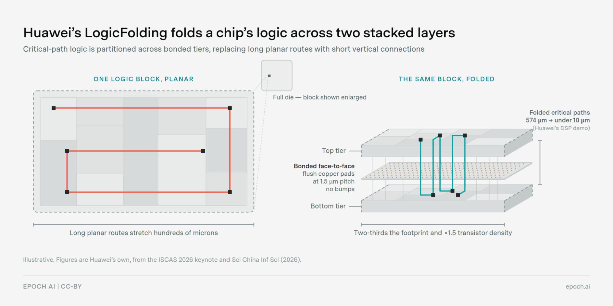
Its plan is to stack logic dies vertically in order to improve transistor density and scale beyond the limits set by its lack of access to advanced lithography tools. The transistors themselves remain 5–7 nm-class devices, distributed across two or more logic layers. Huawei calls this 3D stacking technique “LogicFolding” and successfully implementing and scaling it is key to Huawei’s competitiveness beyond 2030.
Benefits of 3D stacking
Vertical stacking offers three benefits.
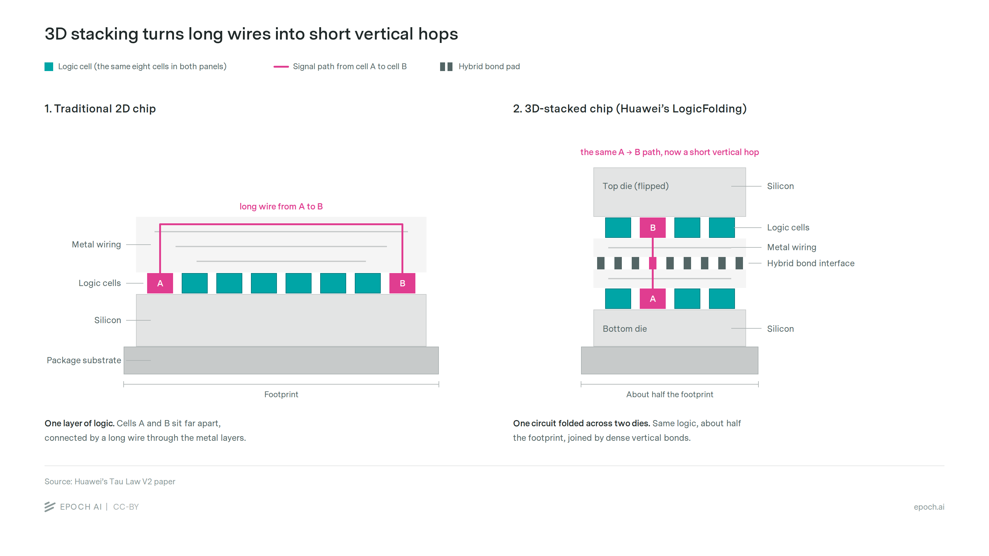
First is increased density. By 2031, Huawei aims to stack two 5 nm-class logic dies in order to achieve the equivalent transistor density of a 1.4 nm process node. While this would greatly increase the arithmetic performance of the Ascend chips, the resulting chip would still trail a planar 1.4 nm process in power efficiency, yield, and cost.
Second is shortening the connections within a chip. A chip can run only as fast as its slowest critical path, so shortening that path can speed up the whole chip. LogicFolding splits a logic block across vertically stacked layers, so some signals travel through the bond as short vertical hops rather than traveling across the face of the die on long horizontal wires. Shorter critical paths also reduce the need for buffers. Buffers are placed along intermediate points on long wires to limit the delay caused by resistance and capacitance. Reducing the number of buffers can save die area and power while also reducing signal delay.
Huawei argues that stacking could have a third effect at the package level: increasing memory and interconnect bandwidth. In a conventional 2.5D AI package, the logic die sits in the center, with HBM stacks and high-speed interconnects around it. The data flowing in and out of the chip must travel through the interfaces at the edges of the logic die. Thus, the rate at which data can be moved to and from the die is tied to the perimeter of the die.
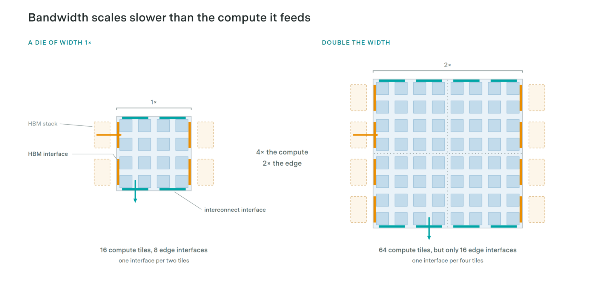
This leads to a geometric mismatch. Compute grows with die area, while the space available for the interconnect and memory interfaces grows with the die perimeter. If the width of a die doubles, its area quadruples while its perimeter only doubles. In other words, compute grows faster than the memory and interconnect bandwidth available to feed it. Huawei calls this the N²-vs-N fan-out dilemma. Stacking logic alone would further this mismatch, since it adds compute without increasing the package-accessible area available for memory interfaces.
Instead of logic on logic, stacking memory on logic could reshape the geometric constraints. Rather than feeding the logic die only through its edges, memory can be bonded directly above or below it and connected across the face of the die using dense hybrid bonds. This allows the area for memory interface capacity to scale with the die area and thus scale at the same rate as compute.
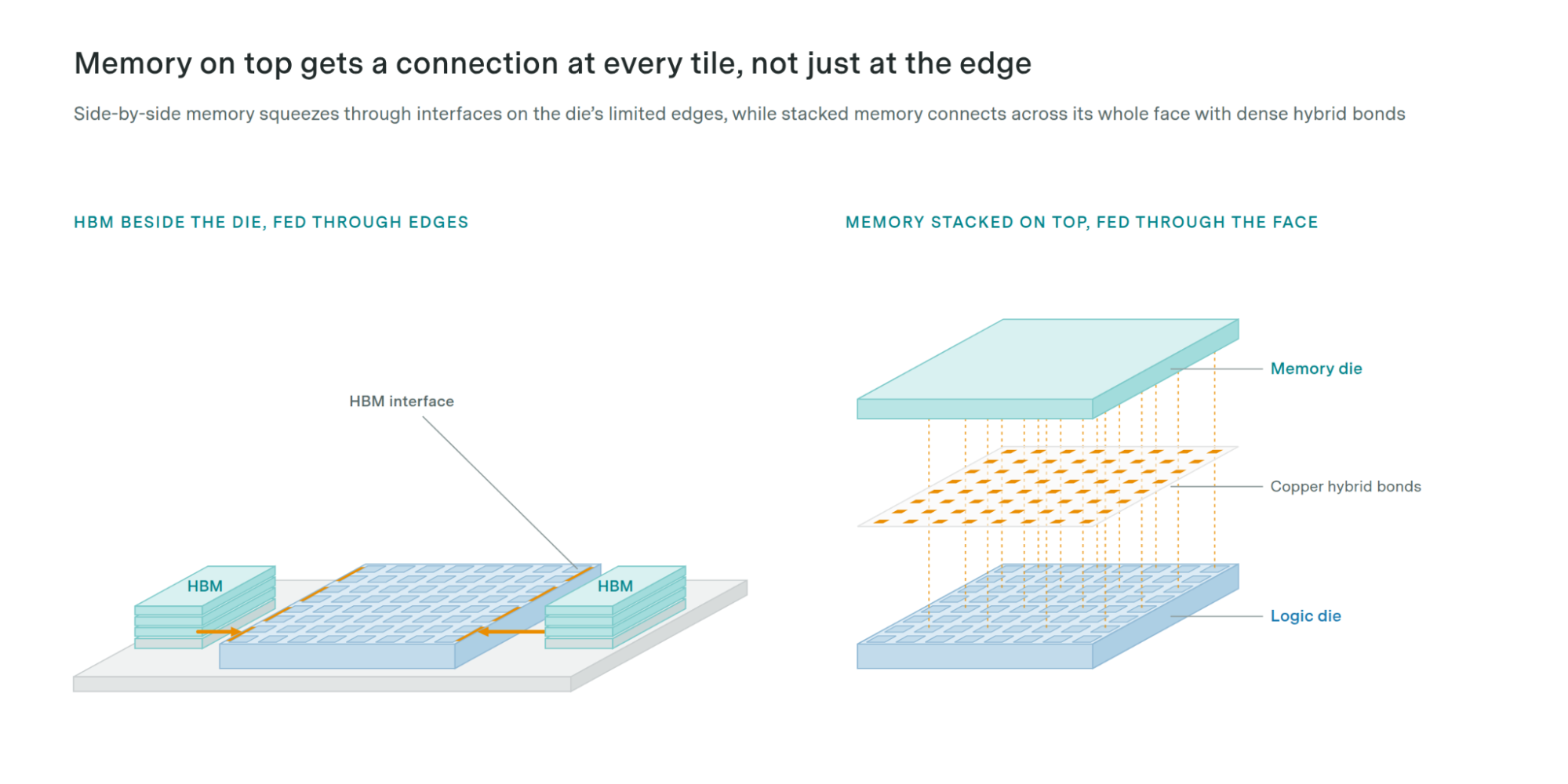
Taken together, Huawei’s bet on 3D stacking attacks Huawei’s per-chip constraints from three points: it increases the amount of compute within a given footprint, reduces the distance some signals travel within a chip, and increases memory and interconnect bandwidth. Read more about the technical challenges of 3D stacking
Huawei and its manufacturing partners will have to address many technical challenges in order to scale 3D stacking.
Stacking vertically is a difficult manufacturing process. When two dies are stacked one on top of another, every signal that passes between them needs a physical connection across the interface where they meet. To have the separate dies function as a single chip, those connections need very high bandwidth and very low latency. If they are too sparse or slow, communication overhead grows and utilization falls.
The manufacturing process for connecting vertically stacked layers relies on hybrid bonding. Traditional 3D stacks such as HBM connect layers with tiny solder microbumps, but those connections are too large and sparse for splitting timing-critical logic across tiers. Relative to microbumps, hybrid bonding allows for far more connections within the same area by joining copper pads directly to one another. The dense interface reduces the time and energy required to move signals between the tiers, and allows LogicFolding to divide a logic block across two dies without communication becoming a severe bottleneck.
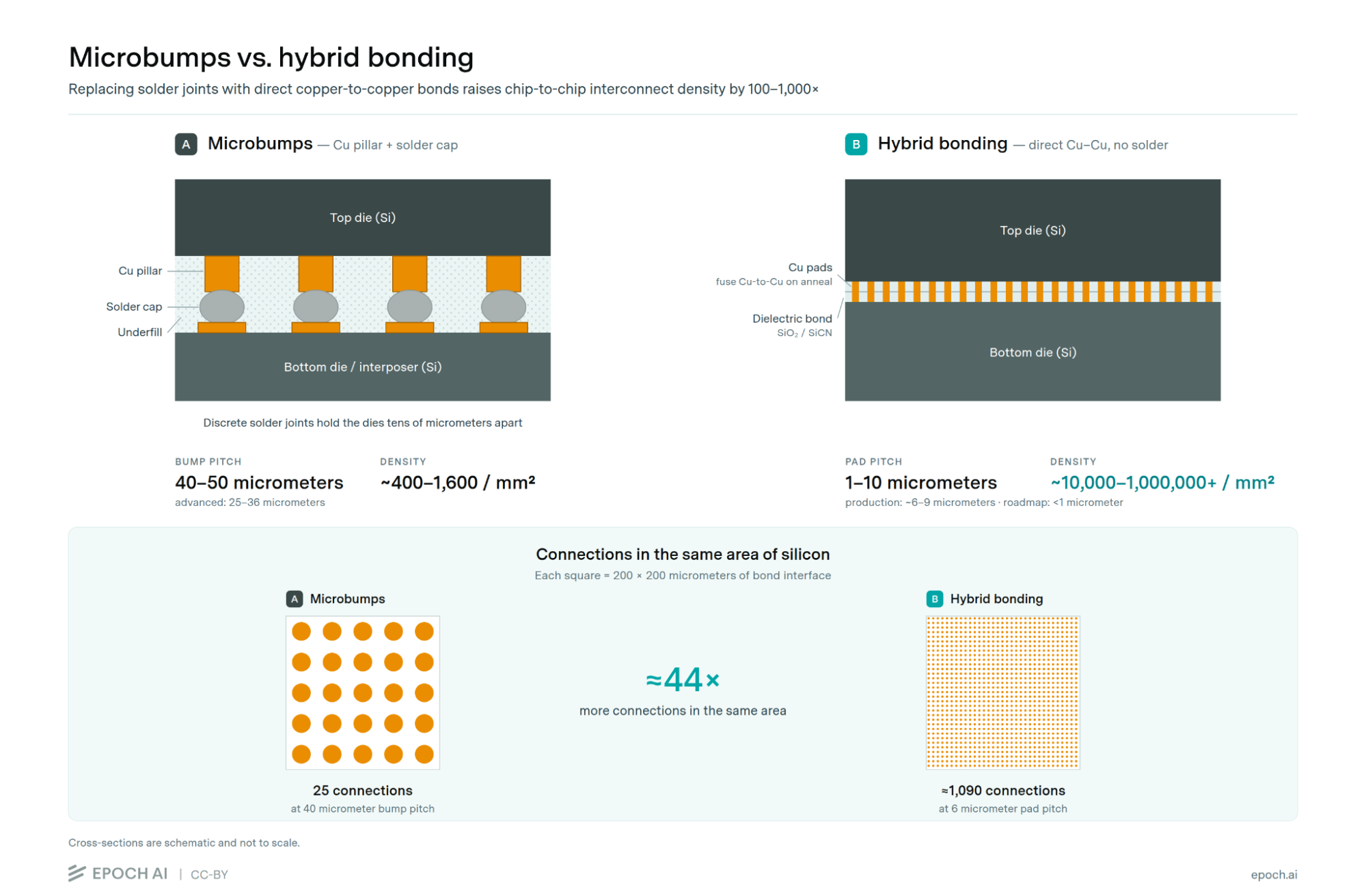
For Huawei, the challenge will be scaling from folding a small chip to a large, power-hungry AI chip. The many challenges of 3D stacking, including yield, alignment, cooling, power delivery, warpage, testing, and design complexity, all worsen as each layer becomes larger and more layers are added. Stacking past two layers is particularly difficult since it compounds yield loss, thermal, and power delivery challenges and could require greater through-silicon via (TSV) density.
China’s relative strength in packaging
The packaging process for connecting vertically stacked layers relies on hybrid bonding. While hybrid bonding is challenging, it fits Huawei’s constraints. Packaging is a strength for China. For decades, semiconductor assembly and packaging have been outsourced to firms including JCET, Tongfu, and Huatian, allowing them to build expertise and scale. China isn’t starting from scratch on hybrid bonding either: YMTC, a Chinese memory manufacturer, already uses it for its NAND products. But stacking relatively cool, defect-tolerant memory is much easier than stacking active logic. The uncertainty is whether Huawei can bond two Ascend dies and whether that process can run at high yield and high volume by the end of the decade.
China also has reasonable access to the necessary tools for hybrid bonding, including wafer bonders, aligners, and chemical mechanical planarization equipment, much of which is not explicitly covered by US export controls. This relative access to the key tools likely played a role in Huawei viewing LogicFolding as a tractable bet.
LogicFolding roadmap
Importantly, the Ascend line is not expected to utilize LogicFolding until 2030. Until then, Huawei will apply LogicFolding to several generations of its Kirin smartphone chips, allowing the process to mature.32
| Year | Chip | Folding |
|---|---|---|
| 2025 | Ascend 910C | None |
| 2026 | Kirin / Mate 90 | 2 layers, partial |
| 2026 | Ascend 950 | None |
| 2027 | Ascend 960 | None |
| 2028 | Ascend 970 | None |
| 2029 | Ascend 980 | None |
| 2030 | Ascend 990 | First Ascend with LogicFolding |
Compared to an Ascend die, a smartphone chip is a far gentler starting point, and Huawei’s results for the folded 2026 Kirin chip demonstrate the benefits of LogicFolding. Huawei reports a 54% increase in density, a 41% reduction in power, and a 13% increase in peak clock speed.33 From here, Huawei’s plan is to keep iterating on the phone chip over three more generations, allowing the LogicFolding process to mature. Read more about Huawei's near-term roadmap for LogicFolding
The die of a smartphone chip is small. Small dies catch fewer defects, so stacking two of them is a survivable yield problem. For example, the Kirin 9020 is a 137 mm² die. Assuming the Kirin chip yields at 70%, the same defect density would imply a yield of 12% for an 800 mm² die. A stack requires at least two good dies, which compounds the penalty: half of the two-die stacks built from Kirin dies would be successful, compared to about 1% of the stacks built from 800 mm² dies. At the same defect density, the Kirin chip would have 30× the production throughput of a reticle-sized Ascend chip. And this is even before accounting for bonding failures.
A smartphone chip is cool, drawing perhaps 10 W, making heat dissipation far more manageable than the hundreds of watts of an Ascend chip. Huawei’s phones also ship in the tens of millions, providing the hybrid bonding line with the volume it needs to move up the yield learning curve.
Huawei’s Kirin density roadmap suggests a step change in 2031. It counts stacked transistors against the chip’s 2D footprint, which rises from 155 million transistors per mm² (MTr/mm²) in 2025 to 238 million in 2026, a 54% jump with the first two-layer fold. The curve then rises slowly by roughly 5% a year, reaching 292 million by 2030. One explanation for the slowdown in transistor density that Huawei projects is that two layers of the 5–7 nm-class logic can hold at most twice the planar figure, roughly 310 MTr/mm², and so the years between 2026 and 2031 are spent stacking more of the die across two layers.
From 2030 to 2031, the density jumps from 292 to 400 MTr/mm². Huawei expects LogicFolding eventually to expand to three or more active tiers, but it doesn’t say how many tiers it plans at each point on the roadmap. However, the sharp jump in 2031 could be due to adding more layers, applying folding across more of the die, using denser cell layouts, improving routing, or a combination of these changes.
Nvidia will stack denser dies sooner
With LogicFolding, Huawei could keep pace through 2030 with the planar transistor density achieved by TSMC’s leading-edge nodes.
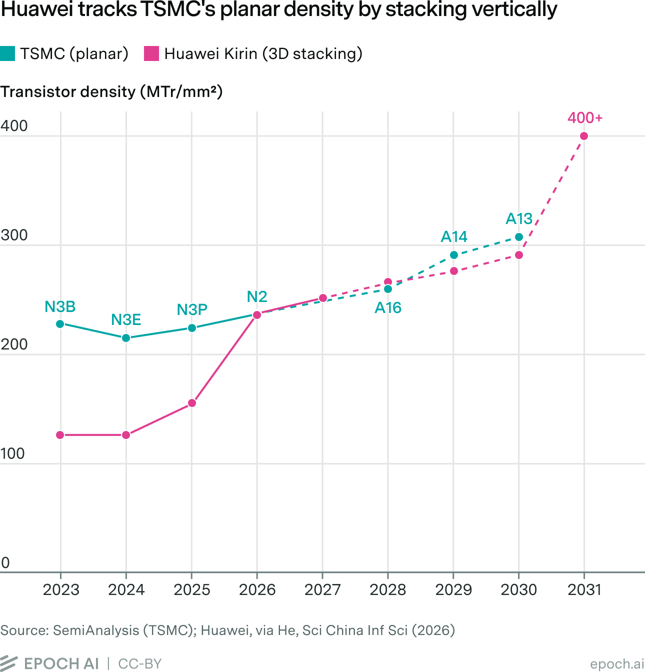
But none of the Ascend chips before 2030, from the 950 through the 980, will use 3D stacking, and the 1.4 nm-equivalence target for 2031 still depends on significant advances in yield, tooling, EDA, and memory that have not yet materialized. Until then, the more traditional methods of scaling chip performance will have to carry Huawei’s Ascend ambitions. Even if Huawei achieves 1.4 nm-equivalent density in 2031 through 3D stacking, Nvidia’s Feynman applies a similar technique on a 1.6 nm process two years earlier.
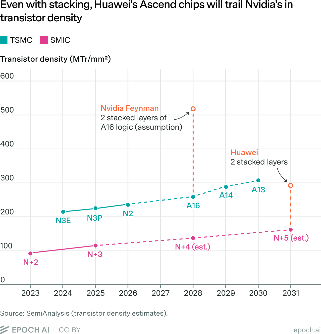
LogicFolding is critical to Huawei’s long-term success. It could help Huawei break through both the compute and memory walls by increasing compute performance beyond the limits of a 5 nm-class process and raising memory bandwidth by stacking memory directly above compute units. But with LogicFolding only coming to the Ascend line in 2030, Huawei’s per-chip performance disadvantage will continue to constrain its total compute output even as China’s HBM capacity expands.
Huawei will likely continue to trail
Huawei began 2026 producing roughly 25× less AI compute than Nvidia. Its chips are three to four years behind, and the supply chain that produces them cannot match Nvidia’s.
Behind much of Huawei’s disadvantage are export controls, which act on both dimensions of competition at once: on volume, through HBM and lithography access, and on performance, through the process node Huawei’s chips are built on. While not stopping Huawei’s progress entirely, export controls have made it far harder, slower, and more expensive for Huawei to compete.
Meanwhile, Nvidia is compounding its lead. Nvidia’s HBM suppliers — SK Hynix, Samsung, and Micron — will spend hundreds of billions of dollars through 2030 building fabrication plants. Nvidia’s Feynman is likely to deliver a significant performance boost over Rubin, and by 2030 Nvidia could even start shipping Feynman’s successor.
Huawei is one of the world’s most capable engineering organizations, and it may eventually catch up — by outperforming Nvidia on vertical stacking, improving its software dramatically enough to close the utilization gap with CUDA, gaining access to a cutting-edge process node, and significantly scaling production. But overcoming these disadvantages will take time, and the available information suggests it’s unlikely to happen by 2030.
Acknowledgements
Thanks to Jack Freed, Hamish Low, Saif Khan, JS Denain, Isabel Juniewicz, and Josh You for their helpful feedback. Special thanks to Irene Trotta for creating the figures and visuals, and to Elliot Stewart, Lynette Bye and Sumiko Neary for editing.
Appendix
Appendix: China’s access to the necessary tools
-
While Huawei currently has the largest share of China’s AI chip market among domestic chip designers, other promising Chinese companies, such as Cambricon, are also emerging.

-
The 950PR more closely resembles Nvidia’s RTX Pro 6000 Blackwell than the B300. The RTX Pro 6000 has similar specs at 2 PFLOPS of FP4 performance and 1.6 TB/s of GDDR7 bandwidth, making it better suited for compute-bound prefill. A better comparison to the B300 is the Ascend 950DT. Huawei uses the same compute die for both 950 variants, but packages the 950DT with 144 GB of its “HiZQ 2.0” memory that provides 4 TB/s of bandwidth. The higher bandwidth of the 950DT makes it more comparable to the B300. It wouldn’t be surprising if US AI labs are disaggregating inference workloads and using the RTX Pro 6000 for the prefill portion.
-
Huawei also focuses on ease of programmability with the 950. Earlier Ascend chips ran SIMD code, which is efficient in silicon but hard to program and incompatible with software written for Nvidia GPUs. The 950 adds hardware support for SIMT, the execution model CUDA is built on, and spends die area on it even as it shrinks total die area.
-
In 2024, Huawei successfully circumvented US export controls and purchased roughly $500 million of 7 nm wafers from TSMC through a shell company, Sophgo. It was also able to stockpile 13 million HBM stacks in the last few months of 2024, before the US export controls on HBM went into effect in January 2025.
-
The stockpile estimate starts from roughly 13 million HBM stacks (16 GB each) accumulated before the Dec 2024 export controls. We assume 80% flowed to Huawei, and subtract the memory already consumed by Huawei’s late-2024 and 2025 production: roughly 300,000 910Bs at 64 GB and 610,000 910Cs at 128 GB, at an 80% packaging yield. We estimate the remaining Huawei stockpile entering 2026 supports the production of 280,000 910Cs.
-
Our smuggling estimate is highly uncertain and speculative. Two Samsung distributors, CoAsia and Faraday, are allegedly engaged in smuggling HBM to China. Each publishes monthly revenue filings and analysts speculate that sharp increases in CoAsia’s and Faraday’s revenues are due to them selling restricted HBM to China. In order to estimate smuggling volumes, we treat excess revenue above the baseline as revenue from smuggling and convert revenue to GB at an assumed $15 per GB. We assume 80% of smuggled HBM goes to Huawei, in line with its share of domestic AI compute production. Each memory channel is assigned to the chip based on whether the specs are compatible. The stockpile is HBM2E, which maps onto the 910C: 16 GB, 8-hi stockpile stacks don’t fit with the specs of the 96 GB 950DT, whose four HBM sites each require a 24 GB stack. The 950DT, with roughly 4 TB/s of memory bandwidth, needs HBM3-class memory or better, so it draws only on the channels that supply it: domestic CXMT and XMC output, plus smuggled HBM, which we assume was HBM3 or HBM3E in both 2025 and 2026. We therefore model smuggled HBM in 2025 feeding into that year’s 910C production, preserving about 150,000 chips’ worth of stockpile for 2026, which lifts the 910C total from 280,000 to 430,000. The 2026 smuggling flow converts to 78,000 units of the 950DT 96 GB variant. Our estimate of smuggling is highly speculative, so it should be treated as a scenario rather than a point estimate.
-
Our model and input parameters are accessible.
-
It is possible that Feynman would stack two dies that each use a different process node, which isn’t uncommon. AMD’s MI450X stacks an N2 die on top of a N3P base die. However, for the sake of this analysis we’ll assume both layers are on a 1.6 nm process.
-
Details such as the number of memory modules, pin transfer rate, bus width, etc are unknown, making it difficult to say with certainty which equivalent generation of HBM the Ascend 970 will utilize.
-
Google also builds pod scale solutions that connect 9,216 of its TPU v7 Ironwood chips. However, the topology is different. Google uses a 3D torus topology, with 64-chip cubes connected through reconfigurable optical circuit switches, rather than Nvidia’s relatively small high-bandwidth switched domain or Huawei’s larger hierarchical fabric. The torus makes very large optical systems economical, but communication overhead depends more heavily on where processors sit in the topology and how workloads are mapped onto it.
-
Ascend 910C, per NPU package. SemiAnalysis states 400 GB/s, Huawei’s paper gives 196 GB/s/die over a dual-die package (~392 GB/s). Both unidirectional, ~10% apart. This is below Blackwell’s 900 GB/s, which is SemiAnalysis’s own comparison.
-
Ascend 950 - Huawei advertises 2 TB/s, which is likely bidirectional. Huawei states it as “2.5× the Ascend 910C”, and the 910C has 400 GB/s unidirectional scale-out bandwidth per-chip.
-
Ascend 960DT. Huawei lists a 2.2 TB/s bidirectional interconnect per chip (Tom’s Hardware), so ~1.1 TB/s unidirectional.
-
Unidirectional bandwidth. Nvidia advertises 1.8 TB/s (Blackwell) and 3.6 TB/s (Rubin) as bidirectional per-GPU NVLink, so half is 900 GB/s and 1.8 TB/s.
-
The Rubin system was announced as “NVL144” at GTC 2025 (counting dies) and renamed “NVL72” in 2026 (counting packages).
-
In networking terms, the bisection bandwidth (the data rate available when the system is split in half and one half sends as much data as possible to the other) meets or exceeds the aggregate injection of the GPUs in one half.
-
Technically, it is 100 GB/s per network interface card.
-
It would in any case be limited by how quickly each GPU can send data to the network through PCIe or chip-to-chip links.
-
Huawei uses a protocol called UnifiedBus that orchestrates communication at the hardware level. Typical pod-scale systems run several networks, each operating at a different layer, which requires handoffs and translating between formats. UnifiedBus claims to replace this and instead run a single protocol, but that claim shouldn’t be taken literally as one uniform connection extending arbitrarily. Huawei still uses different links, switches, and network layers at different distances, and its current systems retain separate UB, RDMA, and conventional Ethernet networks for different types of traffic. UnifiedBus unifies how resources inside its domain are addressed and used, but it doesn’t make the distance between any pair of chips equivalent.
-
For example, SemiAnalysis measures that a GB300 NVL72 rack at ~35 tokens per second per user delivers 1,920 tokens per second per GPU under Dynamo vLLM, compared with 9,228 under Dynamo SGLang. The difference in token throughput is nearly 5×. Adding other inference optimizations such as multi-token prediction can increase throughput further, in some cases by over an order of magnitude.
-
Huawei is trying to expand the developer ecosystem for Ascend as well. It has open-sourced many of the CANN components, and is integrating Ascend with tools such as PyTorch, Triton, and vLLM, and has committed tens of thousands of its GPUs to the ecosystem. This lets developers modify the lower-level software themselves, and wider access to Ascend gives more people the opportunity to find and fix its weaknesses.
-
Much of the Ascend production to date has relied on foreign components. A teardown reportedly found that the Ascend 910C parts use TSMC logic and Samsung or SK Hynix HBM rather than fully domestic silicon. Even if Huawei hits the performance targets on its future Ascend roadmap, it remains an open question whether China’s domestic supply chain can provide the key components at the scale needed to produce millions of Ascend units.
-
For our estimates through 2028, we assume HBM remains the binding constraint on Ascend production. However, if advanced packaging or logic supply binds first, these figures would still be meaningful as upper bounds on domestic output.
-
These two assumptions together cut Huawei’s estimated 2026 output using domestic HBM by 4×.
-
According to Huawei’s documentation, the 950DT contains four HBM stacks, and the lower-capacity version is unlikely to result from one module being defective, since that would give 108 GB and reduce bandwidth to 3 TB/s. Rather, the lower capacity likely comes from shorter stacks on the same interface: four 8-high stacks rather than four 12-high stacks. This better matches CXMT’s current capabilities since it is more likely to be mass-producing 8-high HBM stacks than 12-high stacks.
-
SemiAnalysis estimates imply that CXMT will allocate 8.6% of its DRAM wafer capacity to HBM in 2026, rising to 13.1% in 2027 and 20% in 2028. Extrapolating that trajectory would put the share at roughly 26% in 2029 and 32% in 2030.
-
This BOTEC is rougher than our other volume estimates since the Ascend roadmap could change substantially by 2030. We assume that in 2030 Huawei will only make the Ascend 980 chip, which has a targeted performance of 28 PFLOPS at FP4 and 384 GB of HBM.
-
Yields in converting DRAM wafers into HBM stacks and integrating them into finished chips.
-
The decomposition also highlights the sensitivity to how we measure AI compute production. The H100-equivalent metric looks at the ratio of peak performance between chips, but it doesn’t account for memory, interconnect, workload shape, interactivity, and other factors, each of which can move observed chip performance significantly.
-
We assume that the Rubin Ultra will pack the same amount of logic as Rubin, but run at a slightly higher clock speed, resulting in the performance bump from 35 PFLOPS to 38 PFLOPS. This is speculative and an uncertainty we capture in the confidence intervals we report.
-
The 31 TB/s memory bandwidth estimate for the 2028 Rubin Ultra assumes that the chip will have 8 stacks of HBM4E at 15 Gb/s per pin.
-
Even on the relatively forgiving Kirin smartphone die, Huawei only folds the most critical parts rather than the whole chip — a sign of how difficult the process is.
-
However, the gains describe two different configurations. The 41% power saving is measured with the folded chip slowed to 2.5 GHz and run at 0.9 V, against the prior chip at 2.75 GHz and 1.1 V, at what Huawei calls equal performance. The 13% clock gain is measured at the full 1.1 V. The chip runs at one point or the other, so the headline figures are trade-offs rather than a single combined gain.